


![]()
Industry’s first * 1 High resolution with high resolution up to a very bright scene (450,000 saturated electrons) Realizing high-quality shooting without motion distortion
Developed 8K high resolution, high performance global shutter imaging technology with CMOS image sensor using organic thin film
* 1: According to our company on February 14, 2018
【Abstract】
Panasonic Corporation is capable of reading images at a high frame rate of 60 fps, high saturation of 450 thousand electrons and global shutter [1] with sensitivity modulation function, achieving 8 K image quality with a high resolution of 36 million pixels We have developed a CMOS image sensor technology. In the present technology, a laminated structure is provided in which an organic thin film that carries out photoelectric conversion and a circuit part that performs charge accumulation and reading are completely independent, and a high-speed noise cancellation technique and a high saturation technology are newly developed and mounted in this circuit part It is. In addition, by realizing the global shutter function using the configuration unique to an organic sensor that can control the voltage applied to the organic thin film and change the sensitivity, these performance are simultaneously realized for the first time in the industry * 1 .
【effect】
With this technology, it is possible to shoot at 8 K high resolution even in scenes with a large contrast difference such as a strong sunlight field and a shaded spectator seat in the stadium, for example.
In addition, taking advantage of the global shutter function, images are taken synchronously between cameras in instantaneous cutout of moving objects without distortion, multi-viewpoint imaging using multiple cameras, and machine vision · ITS It is expected to be applied to fields requiring high speed and high resolution such as monitoring.
In addition, it is necessary to manually or mechanically attach the ND filter [3] which is conventionally different for each photographing condition by utilizing the function that can be subjected to sensitivity modulation [2] only by controlling the voltage applied to the organic thin film by this sensor , We can realize the ND filter function that can adjust the sensitivity steplessly only with voltage control even in the scenes where we needed it.
【Features】
This development has the following features.
1. Simultaneous realization of 8 K resolution, 60 fps frame rate, 450 thousand electron saturation, global shutter function.
2. Switching between high sensitivity mode and high saturation mode can be switched by using the gain switching function.
3. By controlling the voltage applied to the organic thin film, ND filter function can be realized steplessly.
【Contents】
This development is realized by the following technology.
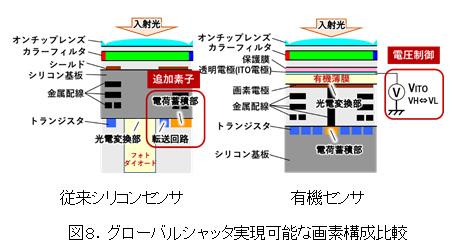
(1) “CMOS image sensor design technology” completely independent of the organic thin film having the photoelectric conversion function and the circuit part for reading the charge accumulation and the photoelectric conversion signal
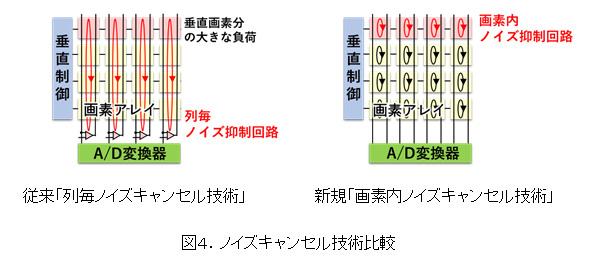
(2) “In-pixel-capacitively coupled noise cancellation technology that can suppress pixel noise at high speed even at high resolution”
(3) “In-pixel-gain switching technology” capable of achieving high saturation characteristics
(4) “Voltage control sensitivity modulation technology” which can change the sensitivity only by changing the voltage applied to the organic thin film
Conventional example
In the conventional global shutter sensor, it was necessary to provide the photodiode and the charge storage capacity in the same pixel, so there was a problem in realizing both high resolution and shooting characteristics in bright scenes.
【Patent】
135 cases in Japan, 83 cases in foreign countries (including pending)
[Remarks]
Part of this technology will be announced at the International Solid-State Circuits Conference (ISSCC) 2018 held in San Francisco, USA from February 11th to February 15th, 2018.
【Contact Information】
- Panasonic Corporation Corporate CTO Office Public Relations
- Email: [email protected]
【Detailed description of content】
1. An organic thin film having a photoelectric conversion function and a circuit section for reading charge accumulation and photoelectric conversion signals are completely independent “CMOS image sensor design technology”
Our organic CMOS image sensor has the function of converting light into electric signal by organic thin film and the function of accumulating and reading out signal charge is done completely independently in the lower layer circuit part respectively. By taking advantage of the structural features of such an organic CMOS image sensor, it is usually a trade-off by mounting a high-speed noise cancellation technique and a technique to realize high saturation in a circuit portion having a high degree of freedom of arrangement , Reading at a frame rate of 60 fps at 8 K high resolution, realization of high saturation characteristics, wide dynamic range [4] , global shutter function at the same time.
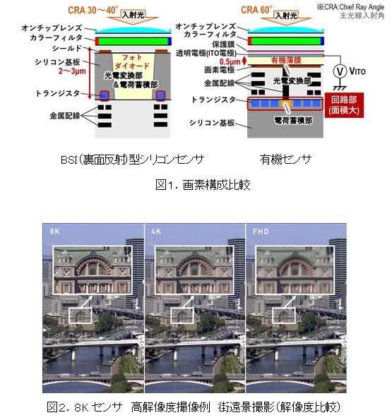
2. “In-pixel-capacitively coupled noise cancellation technology that can suppress pixel noise at high speed even at high resolution”
Since the organic CMOS image sensor has a structure that connects the organic thin film and the charge accumulation part with metal wiring, accumulated charge can not be completely read out. Therefore, there is a problem that it is affected by reset noise at the time of resetting the pixel (signal charge storage node). Furthermore, with a multi-pixel sensor such as an 8K sensor, it was necessary to drive large loads exceeding 4000 pixels aligned in the vertical direction at the same time at the time of noise cancellation, and there was a problem that it takes time to suppress noise. In this sensor, we developed a configuration that cancels the reset noise generated by our proprietary semiconductor device technology and the newly developed “intra-pixel-capacitively coupled noise cancellation circuit” at high speed even when driving multiple pixels . In this configuration, by using a negative feedback loop in which all elements except the current source are provided in the pixel, reset noise suppression can be realized at high speed for each pixel.
3. “In-pixel-gain switching technology” capable of achieving high saturation characteristics
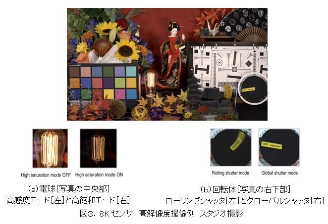
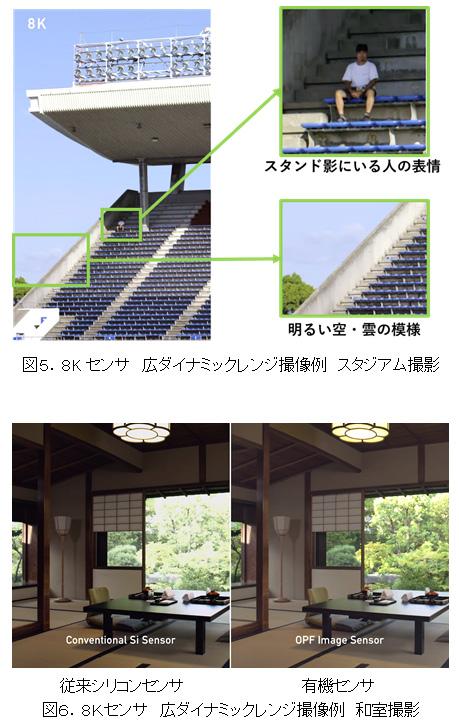
In an organic CMOS image sensor, by mounting a large capacity capacitive element in a circuit portion having a degree of freedom of arrangement, it is possible to switch both the high sensitivity mode and the high saturation mode by using only the switch from the camera system while using the same pixel configuration Mode can be realized. In the high sensitivity mode, it is possible to image data up to the light quantity of 4.5 thousand electrons with high sensitivity. On the other hand, in the high saturation mode, it is possible to capture data up to 450 thousand electrons. In this sensor, it is possible to capture images up to 10 times the high sensitivity mode ratio in the high saturation mode. Therefore, as shown in Fig. 3 (a), in the high sensitivity mode, the white is skipped and the gradation can not be expressed Even fine filament winding structure can be clearly displayed. Also, as shown in Fig. 5, from the expression of the person in the shadow of the roof of the stadium to the blue sky and clouds during midsummer day, and further from the dim room to the sunny garden, as shown in Figure 6, Even in this case, it is possible to shoot brilliant colors with no blackouts and no whiteouts.
4. “Voltage control sensitivity modulation technology” which can change the sensitivity only by changing the voltage applied to the organic thin film
Organic CMOS image sensors can change the sensitivity of organic thin films simply by controlling the voltage applied to the organic thin film. By utilizing this function, we can realize the following functions which could not be realized with conventional silicon image sensor.
Sensitivity modulation Example 1: Global shutter function capable of simultaneous imaging of all pixels at 8 K resolution
By controlling ON / OFF of the voltage applied to the organic thin film and by controlling the sensitivity of the organic thin film, we realize the “global shutter function” which can capture all pixels at the same time even in multi-pixel driving like the 8K sensor. By taking a picture using the global shutter function, as shown in Fig. 3 (b), it is possible to clearly capture the character of the rotating body without distortion. In addition, as shown in Fig. 7, even at the time of high speed moving object imaging such as when driving on a highway or at industrial inspection, imaging without distortion becomes possible.

In the conventional global shutter type silicon image sensor, it is necessary to add a new element such as a transfer circuit and a charge storage capacity for accumulating charges in order to accumulate data all at once in all pixels, and it is necessary to add a photo There was a problem that the coordination of the area of the diode and the additional circuit occurred, the pixel size could not be reduced, and the saturation light amount could not be increased. Meanwhile, in the organic CMOS image sensor, since no additional element is required, it is possible to realize miniaturization of the cell and high resolution sensor, and by installing a saturation expansion capacity in a circuit section having freedom of arrangement, it is very bright from a dark scene Up to the scene, accurate imaging without distortion becomes possible. For example, as shown in FIG. 9 , even in a scene with a high contrast such as a white sky and a blackout in the past, such as a bright sky and a dark window when the building group is subjected to high-speed panning [5] With the organic CMOS image sensor, as with the rolling shutter mode, it is possible to acquire image data without distortion while maintaining the gradation of the whole area.

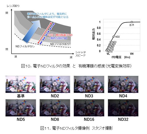
Sensitivity Modulation Example 2: “Electron ND Filter Technology that Can Continuously and Sensitively Change Sensitivity”
By controlling the voltage applied to the organic thin film (VITO in FIG. 8) and changing the sensitivity of the organic thin film to a desired value, conventionally it was necessary to equip a plurality of ND filters according to photographing conditions , It is possible to electrically implement the ND filter function only by controlling the voltage to the camera system. By using this function, it becomes possible to simplify the photographic equipment and to continuously and continuously control the sensitivity which could not be realized with the conventional silicon sensor, so the degree of freedom of shooting according to the scene is expanded.
In the future, we will propose these organic CMOS image sensor technologies to a wide range of applications including business broadcast cameras, surveillance cameras, industrial inspection cameras, car cameras, etc. In order to realize high resolution, high speed and high precision imaging and sensing functions I will contribute.
【Explanation of terms】
- [1] Global shutter
- Shutter operation performed at the same timing of all pixels. In a typical CMOS image sensor, a rolling shutter operation for performing a shutter operation for each row is used.
- [2] sensitivity modulation
- The photoelectric conversion efficiency is to be changed according to the control. In the organic CMOS image sensor, the photoelectric conversion efficiency is made variable by controlling the voltage applied to the organic thin film.
- [3] ND filter
- Abbreviated name of neutral density filter. An optical filter having the function of absorbing evenly visible light in the visible range, and having the function of reducing only the light amount without affecting the color development.
- [4] Dynamic range
- The range of brightness that can be photographed (the ratio of the brightest part to the darkest part).
- [5] Panning
- One of the shooting techniques of video, moving the framing in the horizontal direction while fixing the camera, technology to capture a wide scene.
Via Panasonic