


![]()
World’s first*1 Organic CMOS Image Sensor with Electrically Controllable Near-Infrared Light Sensitivity
The new technology enables frame by frame switching between modes of color imaging and NIR imaging. In addition, fine motion sensing is realized by global shutter operation.
Osaka Japan, – Panasonic Corporation today announced that it has developed a new technology, electrical control of the near infrared (NIR) light sensitivity of the same pixel in an organic CMOS image sensor. The sensitivity of all the pixels in the image sensor, which has directly stacked organic films, is simultaneously controlled by changing the applied voltage to the organic films.
This technology enables to switch between modes of color imaging*2 and NIR imaging frame by frame without a mechanical IR cut filter required for conventional image sensors. This contributes to miniaturizing a camera system and improving the robustness. This technology also enables global shutter operation*3 [1]. Therefore, it can be suitable for applications in various fields of industry such as machine vision or intelligent transportation system, in which fast and accurate inspection or recognition are necessary.
The new technology has the following advantage.
Frame by frame switching between color imaging mode and NIR imaging mode without the loss of resolution.
The development is based on the following technologies.
- The design technology of organic CMOS image sensors which enables to design the photoelectric conversion part and the readout circuit part independently.
- The sensitivity control technology which enables frame by frame switching between color imaging mode and NIR imaging mode by changing the applied voltage to the photoelectric conversion part.
Panasonic holds 94 Japanese patents and 68 overseas patents (including pending) related to these technologies.
Panasonic will present some part of these technologies at the international academic conference: ISSCC (International Solid-State Circuit Conference) 2017 which is to be held in San Francisco on February 5 – February 9, 2017.
Notes:
- *1: As of February 9, 2017, according to Panasonic data.
- *2: The extinction ratio of NIR sensitivity at 800 nm was -28 dB.
- *3: Previous report in ISSCC2016, http://news.panasonic.com/global/press/data/2016/02/en160203-6/en160203-6.html
More on the Technologies
1. The organic CMOS Image Sensor Design Technology, in that, photoelectric conversion part and the readout circuit part can be designed independently.
In the organic CMOS image sensor, photoelectric conversion is executed by an organic film while signal charge accumulation and the signal readout are executed by Si based circuits beneath the organic film. The film and the circuits can be designed independently, so the organic CMOS image sensor can achieve the following features: high sensitivity, wide-dynamic range [2], and global shutter function. The newly developed technology has been realized to extend the spectral sensitivity of the image sensor from visible light spectrum to near infrared (NIR) light spectrum. And also, it makes possible to control the NIR light sensitivity electrically without losing the unique features of organic CMOS image sensors as described above.
2. The Sensitivity Control Technology, in that, frame by frame switching between color imaging and NIR imaging can be realized by changing the applied voltage to the organic layer.
The spectral sensitivity of an organic CMOS image sensor can be extended from visible light spectrum to NIR light spectrum by stacking two organic layers, one of which can absorb visible light and the other of which can absorb NIR light. However, just simply stacking or mixing those two layers does not allow to distinguish the NIR light signal from visible light signal. In order to distinguish those signals, conventional methods need extra components such as electrodes and thin-film transistors, that results in increasing the pixel size.
To solve this problem, we adopted the direct stacked structure of two organic layers with the high resistance ratio of those. In this structure, the applied voltage is distributed to those two layers unequally. In other words, relatively low voltage is applied to one organic layer while relatively high voltage is applied to the other layer using the same voltage source. Organic CMOS image sensors need to be applied the voltage at least higher than a threshold in order to get signal information from incident light. Due to the characteristic, it is realized by the structure that both of those layers have no sensitivity at the low voltage, only one layer has sensitivity at the middle voltage, and both of those layers have sensitivity at the high voltage. Namely, this structure enables electrical switching of color imaging mode, in which the sensor is sensitive only to visible light (shown in left side of Fig. 1) and NIR imaging mode, in which the sensor is sensitive to visible light and NIR light (shown in right side of Fig. 1) without increasing any component.

Fig.1
Cross-sectional image of stacked organic CMOS image sensor with the control of the sensitivity by changing the applied voltage.
The followings are applications of the organic CMOS image sensor design technology and the sensitivity control technology.
Night vision use for surveillance cameras
NIR imaging mode enables to capture clear images even in the too dark situation for human eye to see. This contributes to improve the visibility of captured images by surveillance cameras in the night. And also, color imaging mode enables to obtain RGB color information*4 based on visible incident light with NIR sensitivity being OFF state. These modes can be switched in the same pixel by changing the applied voltage to it, so IR cut filter is not necessary for this image sensor.

Fig.2
Images captured in color imaging mode (Left) and NIR imaging mode (Right).
Notes:
- *4: Fig. 2 is the comparison with monochrome images because the fabricated image sensor in this time has no on-chip color filter.
Non-destructive inspection use
Conventional image sensors which can capture both color images and NIR images without IR cut filter have a specific color filter which substitute NIR pass filter for the one of two green pass filters in the Bayer arrangement [3] color filter. This indicates the pixel count of NIR images is one fourth of total pixel counts in the image sensor. On the other hand, this technology enables to capture NIR images using all pixels on the pixel array in NIR imaging mode. Therefore the NIR images captured by the organic CMOS image sensor do not have the loss of resolution. This feature contributes to improving the accuracy of inspection use, in which NIR images helps to obtain the information inside or backside some materials which transmits NIR light.
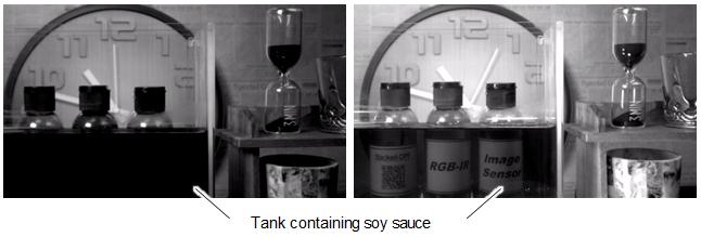
Fig.3
Images captured in color imaging mode (Left) and NIR imaging mode (Right). NIR imaging makes it possible to see characters on the labels of small bottles over a tank filled with soy source.
Machine vision use
The image sensor can be also used for machine vision use. Even through subjects move with high speed and in invisible spectrum range, the image sensor can capture the image clearly. By controlling the sensitivity of the image sensor electrically, frame by frame image capture of subjects in different spectra is realized. This feature makes it possible for machine vison to earn images in both the visible light spectrum and the NIR light spectrum alternately by only a frame.

Fig.4
Frame by frame images of bottles on a rotating table captured when modes of color imaging and NIR imaging are switched by changing the applied voltage to the image sensor’s organic layer. The QR code is printed with a special ink reacting differently for different spectrum, on the bottle’s label. Even in a rotating motion, the organic image sensor with NIR sensitivity can capture the clear image of the QR code on the bottle’s label.
By applying our newly developed technologies, applications in various fields of industry can be realized like night vision, non-destructive inspection, and machine vision.
Technical Terms:
- [1] Global Shutter Technology
- This technology allows to shutter all pixels on an entire pixel array simultaneously.
- [2] Wide-Dynamic-Range Technology
- This technology enables accurate imaging and reproduce of richer color tone, even in high-contrast situations.
- [3] Bayer Arrangement
- One of arrangements used on the pixel array of image sensors.
The pixel array has a repetitive pattern of 2×2 pixels’ group called RGGB.
Via Panasonic