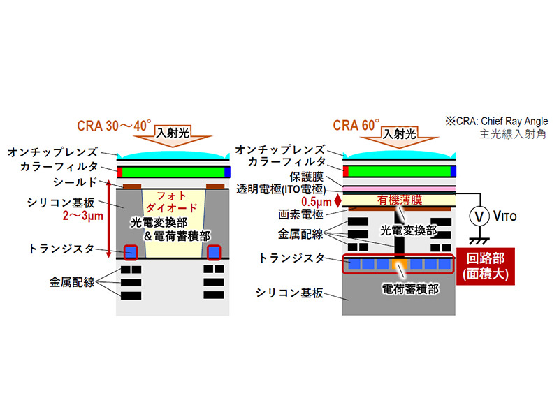
Comparison of pixel configuration with ordinary CMOS image sensor (left)
Translated From DC.Watch
Panasonic Corporation, a high-resolution 36 million pixels that yields an 8K image quality, speed reading frame rate of 60 fps, developed CMOS image sensor design technology capable global shutter imaging with high saturation and sensitivity modulation function of 450,000 electron We announced.
In this technology, the function of converting light into an electric signal is an organic thin film, and the function of storing and reading signal charges is completely and independently performed in the lower layer circuit section.
These, taking advantage of the structural features of organic CMOS image sensor, mounting the freedom of arrangement of the larger circuit unit to realize high speed noise canceling technology and high saturation in the art, in 8K high resolution typically as a tradeoff 60 fps read out, wide dynamic range by realizing high saturation characteristics, global shutter function for the first time in the industry simultaneously realized.
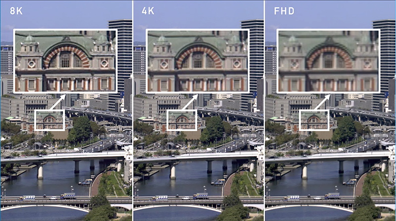
8K sensor High Resolution Imaging Example City Landscape Photography (Resolution Comparison)
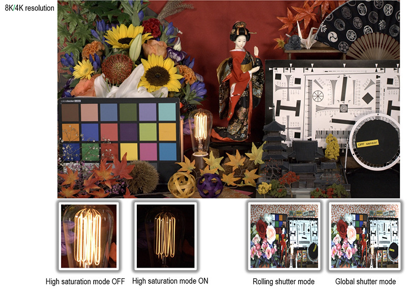
8K sensor High resolution shooting example Studio shoot
In-pixel – capacitively coupled noise cancellation technology
Since the organic CMOS image sensor has a structure in which the organic thin film and the charge accumulation portion are connected by metal wirings, accumulated charge can not be completely read out. Therefore, there is a problem that the pixel (signal charge storage node) is affected by the reset noise at the time of resetting. Further, in a multi-pixel sensor such as an 8K sensor, it is necessary to drive large loads of more than 4,000 pixels aligned in the vertical direction at the same time at the time of noise cancellation, and there was a problem that it takes time to suppress noise.
The company developed a configuration that cancels the reset noise generated at high speed even when driving multiple pixels by using original semiconductor device technology and a newly developed “intra-pixel-capacitively coupled noise cancellation circuit”. In the same configuration, it is said that by using a negative feedback loop in which all elements other than the current source are provided in the pixel, reset noise suppression can be realized at each pixel at high speed.
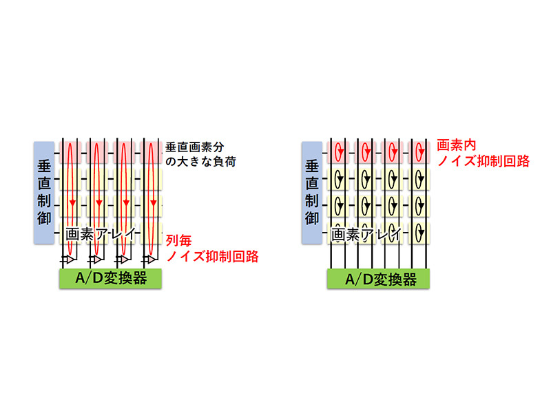
Noise cancellation technology comparison
In-pixel-gain switching technology
By mounting a capacitor of large capacity circuit portion with a freedom of arrangement, while using the same pixel structure, realized only by switching the switching from the camera system as a “high-sensitivity mode” both modes “high saturation mode” .
In high sensitivity mode, 45,000 electronic data up amount is capable of imaging with high sensitivity, the high saturation mode, it is possible to image the data to a large quantity of 450,000 electrons.
In the high saturation mode, it also supports imaging up to 10 times the high sensitivity mode ratio. In the high-sensitivity mode, the white is skipped, and points where gradation can not be expressed also clearly can be displayed.
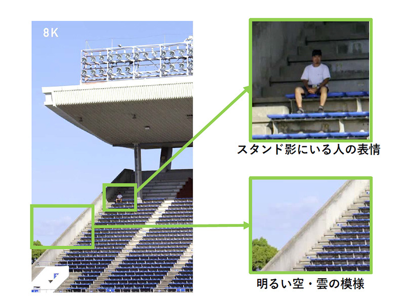
8K Sensor Wide Dynamic Range Imaging Example Stadium Shooting
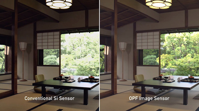
8K Sensor Wide Dynamic Range Imaging Example Japanese Style Photography
Voltage control sensitivity modulation technology
Just by controlling the voltage applied to the organic thin film, it corresponds to sensitivity change of the organic thin film. By utilizing the function, capable of changing all pixel simultaneous imaging possible “global shutter function” and sensitivity in a conventional 8K resolution which could not be achieved by the silicon image sensor in a continuous-steplessly “Electronic ND filter technology” And realized the function.
Global shutter in the function, the character of the rotating body can clearly imaged without distortion, not only imaging with synchronization between the cameras in performing multi-view imaging using a plurality of cameras “multi viewpoint camera” expressway Since imaging without distortion can be obtained even at the time of high speed moving object imaging such as at the time of running or at the time of industrial inspection, it can be expected to be utilized in fields requiring high speed and high resolution.

Comparison between rolling shutter mode and global shutter mode Highway traveling shooting

Comparison between rolling shutter mode and global shutter mode High-speed panning shooting
In the electronic ND filter technology, even in a scene in which it is necessary to equip a plurality of ND filters according to photographing conditions, by utilizing the function capable of sensitivity modulation only by controlling the voltage applied to the organic thin film, We realized an ND filter which can adjust the sensitivity of the ND filter. The same function makes it possible to simplify the photographic equipment which could not be realized with the conventional silicon sensor, and to enable continuous and stepless control of the sensitivity, thereby increasing the freedom of photography according to the scene.
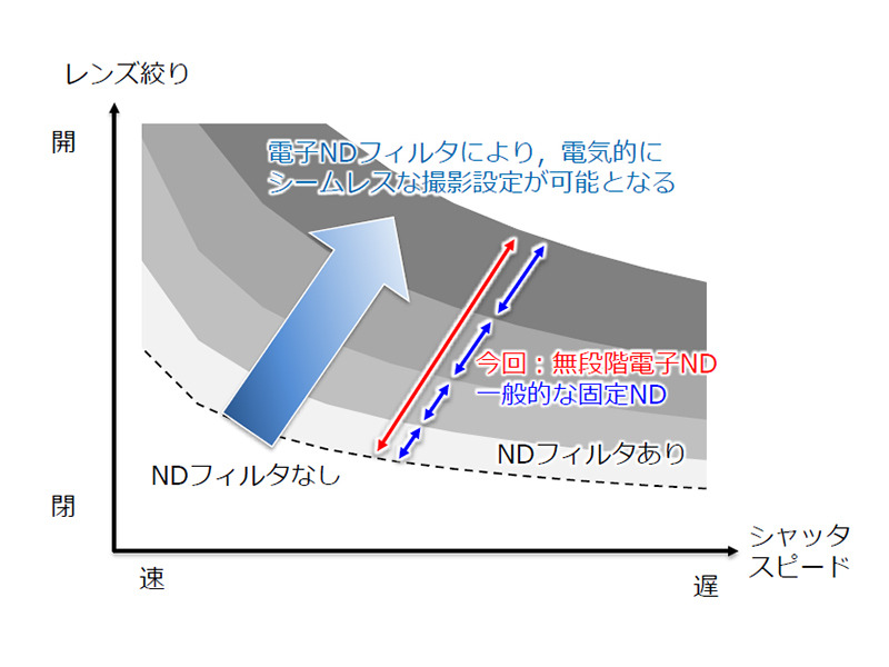
Electron ND filter effect

Electron ND filter image capturing example Studio shooting
The company says to propose organic CMOS image sensor technology to a wide range of applications such as business broadcast cameras, surveillance cameras, industrial inspection cameras, car cameras.
Translated Release via DC.Watch